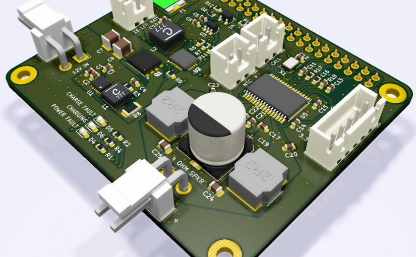
I recently had to design a 4-layer PCB and I finally decided to give KiCad another try (after hearing great things about version 5). I’ve known about KiCad for years and even tried it once a few years back but it never felt quite “there” yet. After spending a few months designing a 4-layer board I have to say it has certainly won me over.
I had to design a fairly complex PCB that included a switching supply, high currents, plenty of thermal vias, high frequency traces, and some mixed-signal work so I was really curious to see what KiCad could do.


One of the most useful features in my opinion is the ability to easily view an interactive 3D rendering of the board with no additional setup. The ability to hide the soldermask and view just the copper layer in the 3D view is a great sanity check on top of the DRC.
Another really really really great feature of KiCad is the ability to easily import any 3D model as an STL or wrl file and visually align and scale it to a footprint. This feature coupled with a site like 3D Content Central that allows you find 3D models from virtually any supplier for free makes accurate PCB design really stress free.

Another underrated KiCad “feature” I have come to love is just how easy it is to move or copy components around in the schematic editor without having to hold down a mouse button. I think this feature, coupled with the convenient shortcuts, saved me quite a bit of time.
Based on this experience I think I’ll definitely stick with KiCad for PCB design until the single license cost for Altium becomes more reasonable. Expect a few detailed KiCad tutorials from me in the near future!

One thought on “4-Layer PCB Design in KiCad 5: Quick Thoughts”